40 pn junction energy band diagram
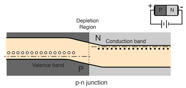
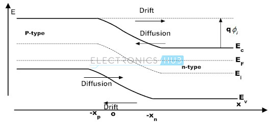
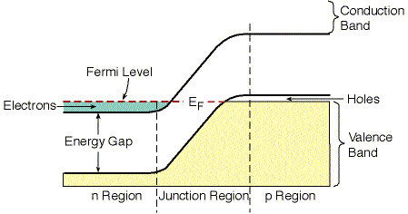
The highest energy band contains valence electrons available for chemical reactions. The conduction band is the band above the valence band. Electrons in the conduction band are free to move about in the lattice and can conduct current. ... P-n junction diffusion and drift Diagram of the diffusion across a p-n junction, with the resultant ... The solid circles on the right of the junction represent the available electrons from the n-type dopant. Near the junction, electrons diffuse across to combine with holes, creating a "depletion region". The energy level sketch above right is a way to visualize the equilibrium condition of the P-N junction. The upward direction in the diagram ...
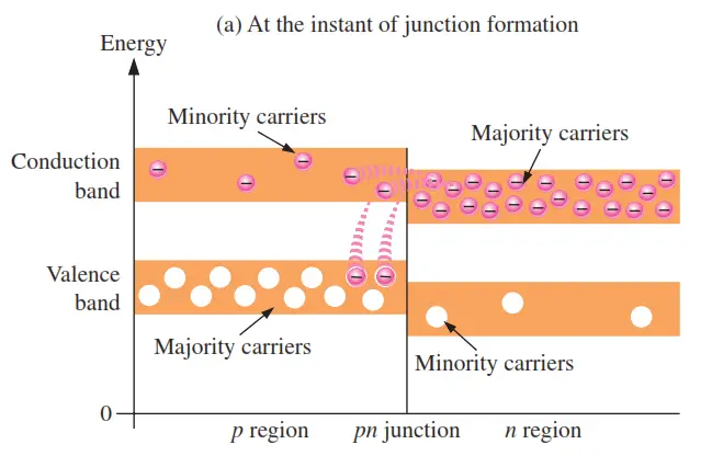
Mar 28, 2019 · The electrons in the conduction band in the energy diagram represent atoms which take part in conduction. The energy gap between the valence and conduction band is called as the forbidden band or band gap. ... The basic components like PN Diode, Bipolar Junction Transistor and Field effect Transistors have their working based on the properties ...
Pn junction energy band diagram
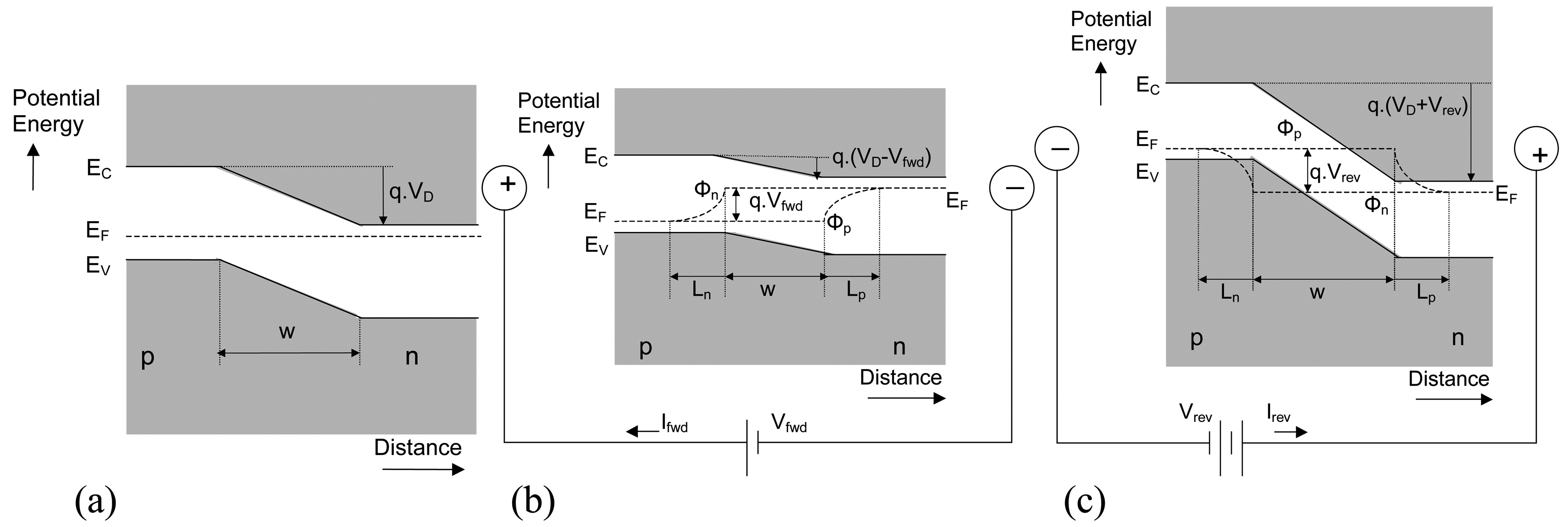
Energy band diagram of a p-n junction (a) before and (b) after merging the n-type and p-type regions Note that this does not automatically align the Fermi energies, E F,n and E F,p . Also, note that this flatband diagram is not an equilibrium diagram since both electrons and holes can lower their energy by crossing the junction. 1 This idealized PN junction is known as a step junction or an abrupt junction. 4.1.1 Energy Band Diagram and Depletion Layer of a PN Junction Let us construct a rough energy band diagram for a PN junction at equilibrium or zero bias voltage. We first draw a … 2.2 A pn Heterojunction Diode Consider a junction of a p-doped semiconductor (semiconductor 1) with an n-doped semiconductor ... of a semiconductor is the energy required to move an electron from the conduction band bottom to the vacuum level and is a material constant. The electron affinity rule ... This is shown in the band diagram below ...
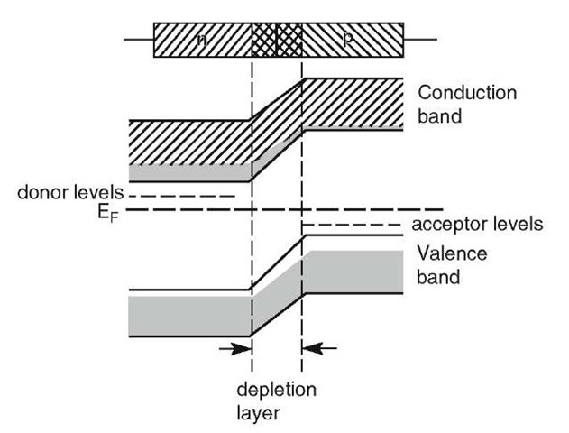
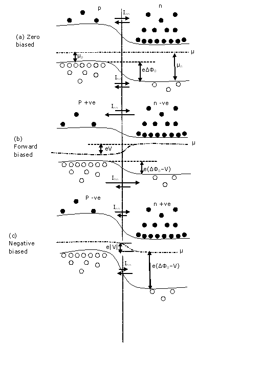
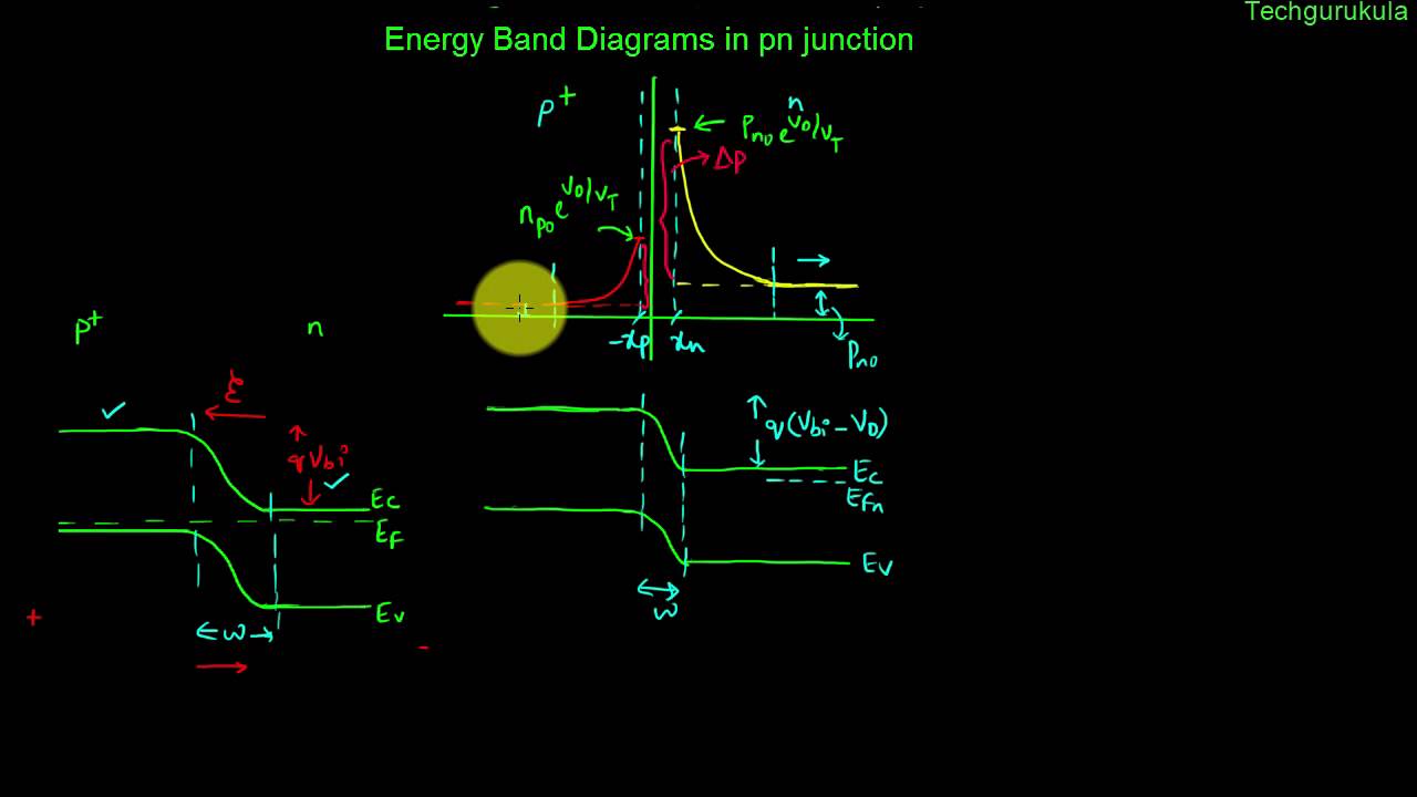
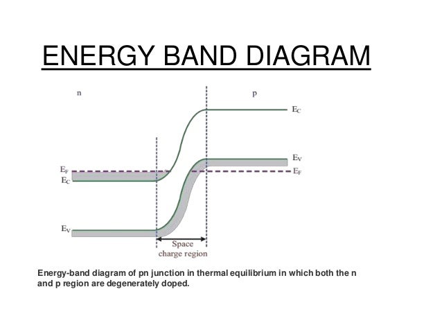
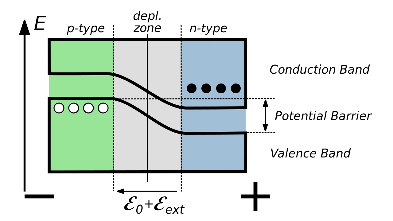
Pn junction energy band diagram. A band gap is the distance between the valence band of electrons and the conduction band.Essentially, the band gap represents the minimum energy that is required to excite an electron up to a state in the conduction band where it can participate in conduction. The lower energy level is the valence band, and thus if a gap exists between this level and the higher energy conduction band, energy ... The panels show energy band diagram, electric field, and net charge density. Both p and n junctions are doped at a 1e15/cm3 (0.00016C/cm 3 ) doping level, leading to built-in potential of ~0.59 V. Reducing depletion width can be inferred from the shrinking charge profile, as fewer dopants are exposed with increasing forward bias. Multi-junction (MJ) solar cells are solar cells with multiple p–n junctions made of different semiconductor materials.Each material's p-n junction will produce electric current in response to different wavelengths of light.The use of multiple semiconducting materials allows the absorbance of a broader range of wavelengths, improving the cell's sunlight to electrical energy conversion efficiency. For a p-n junction at equilibrium, the fermi levels match on the two sides of the junctions. Electrons and holes reach an equilibrium at the junction and form a depletion region.The upward direction in the diagram represents increasing electron energy. That implies that you would have to supply energy to get an electron to go up on the diagram, and supply energy to get a hole to go down.
2.2 A pn Heterojunction Diode Consider a junction of a p-doped semiconductor (semiconductor 1) with an n-doped semiconductor ... of a semiconductor is the energy required to move an electron from the conduction band bottom to the vacuum level and is a material constant. The electron affinity rule ... This is shown in the band diagram below ... 1 This idealized PN junction is known as a step junction or an abrupt junction. 4.1.1 Energy Band Diagram and Depletion Layer of a PN Junction Let us construct a rough energy band diagram for a PN junction at equilibrium or zero bias voltage. We first draw a … Energy band diagram of a p-n junction (a) before and (b) after merging the n-type and p-type regions Note that this does not automatically align the Fermi energies, E F,n and E F,p . Also, note that this flatband diagram is not an equilibrium diagram since both electrons and holes can lower their energy by crossing the junction.
2
Semiconductors Electrical Properties Of Materials Part 3

Energy Diagrams Of The Pn Junction And Depletion Region Electronics 143

Energy Band Diagram In A Pn Junction All About Circuits
Electronic Devices Lecture 35 The Energy Band Diagram Of The Pn Junction Youtube

Basic Electrical And Electronics Engineering Pdf Free Download

File Pn Junction Equilibrium Svg Wikimedia Commons

Video 5 2 Energy Band Diagram Of A Forward Bised Pn Junction Youtube

Semiconductors Electrical Properties Of Materials Part 3
Biasing Of P N Junctions
Simplified Energy Band Diagram Of A P N Junction A At Equilibrium And Download Scientific Diagram

Energy Band Diagram Of P N Junction Diode Lessons Blendspace

Gate Ese Explanation Of Tunnel Diode On The Basis Of Energy Band Diagram Part 2 In Hindi Offered By Unacademy
Energy Diagrams Of Pn Junction Depletion Region Inst Tools

Chapter 4 P N Junction Part I Ppt Video Online Download
P N Junction
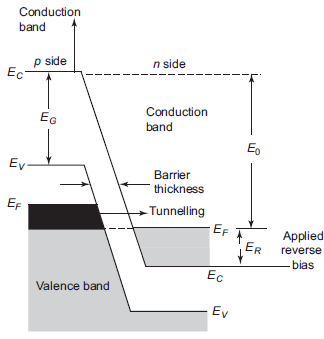
Tunnel Diode Working And Characteristics Electronics Club
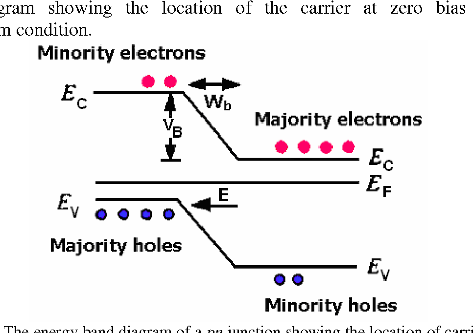
Figure 1 4 From Chapter 1 Semiconductor Pn Junction Theory And Applications 1 0 Introduction 1 1 Pn Junction At Equilibrium Semantic Scholar
Miirbe Energy Band Diagram Of Pn Junction Diode At Equilibrium
Electronic Devices Energy Band Diagrams In Pn Junction With Fermi Levels Youtube

Pn Junction Band Diagram Electronics World
12695 Solid State M Icrowave Devices
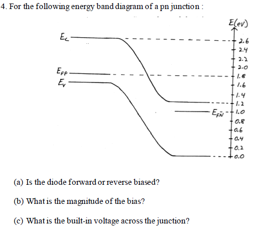
Solved 4 For The Following Energy Band Diagram Of A Pn Chegg Com
In Band Diagram Why The Fermi Energy Ef Is Constant Along The Device Electrical Engineering Stack Exchange
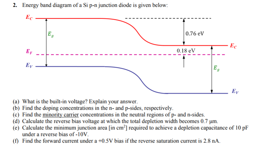
Solved 2 Energy Band Diagram Of A Si P N Junction Diode Is Chegg Com

8 Draw The Energy Band Diagram Of An Unbiased P N Junction And Mark The Barrier Potential And Depletion Region
1

Energy Band Diagram An Overview Sciencedirect Topics

P N Junctions And Band Gaps

How Does A Diode Work Part 1 The Pn Junction Circuitbread

Biasing Of P N Junctions
File Reverse Biased Pn Junction Bands Svg Wikimedia Commons
Sensors Free Full Text P N Junction Photocurrent Modelling Evaluation Under Optical And Electrical Excitation Html

Energy Band Diagram Of Gaas P N Junction In Bulk Continued Lines And Download Scientific Diagram

Energy Gap Of Pn Junction Diode Experiment

Pn Junction Unbiased

Energy Band Diagram An Overview Sciencedirect Topics
Rami Arieli The Laser Adventure
Problem 4 25 Marks The Energy Band Diagram For A Reverse Biased Si Pn Junction Diode Under Steady State Conditions Is Pictured In Fig Course Hero

Unit Ii Zener Diode Breakdown Mechanisms Applications Led
0 Response to "40 pn junction energy band diagram"
Post a Comment