39 mos capacitor band diagram
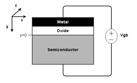
Draw and explain energy band diagram of MOS capacitor in ... Fig1 energy band diagram and MOSFET internal charge distribution in accumulation region Where E C = conduction band energy level E F = Fermi energy level E V = valance band energy level E i = intrinsic energy level Q = charge of electron V g =voltage applied on gate Φ s =surface voltage mosfet - MOS Capacitor band diagram question - Electrical ... MOS Capacitor band diagram question. Ask Question Asked 2 months ago. Active 2 months ago. Viewed 25 times 0 \$\begingroup\$ In a MOS system, is the energy offset between metal/oxide or semiconductor/oxide always the same regardless of the gate voltage applied? In other words, are A and B in the diagram above always the same?
Draw and explain energy band diagram of MOS capacitor in ... The energy band diagram contains the electron energy levels in the MOS structure as deliniated with the fermi energy in the metal and semiconductor as well as the conduction and valence band edge in the oxide and the silicon.

Mos capacitor band diagram
Band-Diagram-of-Ideal-MOS | MOS-Capacitor Digital-CMOS ... Band-Diagram-of-Ideal-MOS MOS-Capacitor Digital-CMOS-Design CMOS-Processing-Technology planar-process-technology,Silicon-Crystal-Growth, Twin-tub-Process, Wafer-Formation-Analog electronic circuits is exciting subject area of electronics. MOS Capacitor With Energy Band Diagrams| CTQ | EC | By G.V ... In Today's video, one of the renowned and experienced faculty of MADE EASY G.V.N Ramesh Sir will help you understand, MOS Capacitor Metal Semiconductor conta... 2-1 MOS Capacitor, MOS Band Diagram - Week 2 | Coursera View Syllabus. From the lesson. Week 2. 2-1 MOS Capacitor, MOS Band Diagram 24:38. 2-2 Threshold Voltage 18:13. 2-3 Realistic Threshold Voltage 21:01.
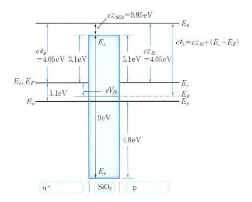
Mos capacitor band diagram. Band-Diagram-of-Nonideal-MOS-with-Bias | Digital-CMOS ... Home > Digital CMOS Design > MOS Capacitor > Band Diagram of Nonideal MOS with Bias. Prev. Next Band Diagram of Nonideal MOS Structure with Bias : we have seen that because of the difference in the work function of both metal and semiconductor there is band bending at the surface of semiconductor. PDF Chapter 1 MOSCap Tool on nanoHUB.org: A Primer Fig. 2. Energy band diagram of an ideal MOS capacitor in equilibrium. 2.1. Operation The simple band diagram as depicted above is modified when a voltage, Vg, is applied on the gate contact. Part of Vg is dropped across the oxide, Vox, and part across the semiconductor, known as the surface potential, φs. PDF Lecture #21 - University of California, Berkeley MOS Band-Diagram Guidelines (cont.) • The barrier height for conduction-band electron flow from the Si into SiO 2 is 3.1 eV - This is equal to the electron-affinity difference (χ Si and χ SiO2) • The barrier height for valence-band hole flow from the Si into SiO 2 is 4.8 eV • The vertical distance between the Fermi level in the metal, E MOS Capacitor Explained - YouTube you want to see more of these videos, or would like to say thanks for this one, the best way you can do that is by becomin...
PDF MOS Capacitor - Chenming Hu It is common to draw the energy band diag ram with the oxide in the middle and the gate and the body on the left- and right-hand sides as shown in Fig. 5-3. The band diagram for V g= 0 (Fig. 5-3b) is quite complex. FIGURE 5-2An MOS transistor is an MOS capacitor with PN junctions at two ends. MOSFET - Wikipedia MOS capacitor. The MOS capacitor is part of the MOSFET structure, where the MOS capacitor is flanked by two p-n junctions. The MOS capacitor is widely used as a storage capacitor in memory chips, and as the basic building block of the charge-coupled device (CCD) in image sensor technology. Chapter51_MOSFET_MOSCap.pdf - Chapter 5 - The MOSFET Metal ... View Chapter51_MOSFET_MOSCap.pdf from ECE 3040 at Georgia State University. Chapter 5 - The MOSFET Metal Oxide Semiconductor Field Effect Transistor 5.1 5.2 5.3 5.4 ... B Ideal MOS Capacitor - TU Wien Ideal MOS Capacitor The band diagrams of an ideal MOS structure consisting of a gate electrode (metal or polysilicon), a dielectric (oxide), and a semiconductor (nMOS or pMOS) are shown in Fig. B.1under different operating conditions for both nMOS and pMOS. For the most simple case it is assumed that (i) there are no
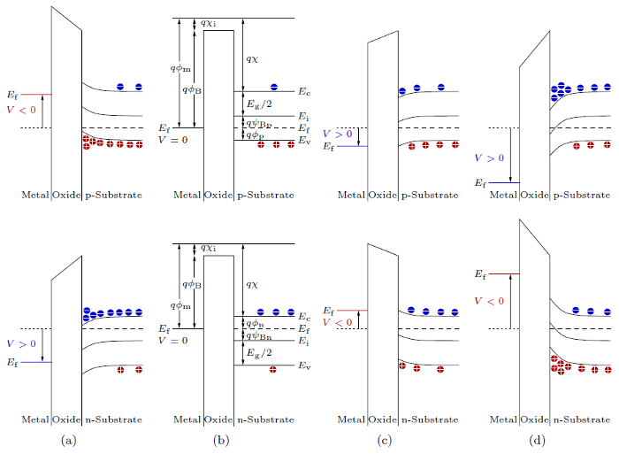
PDF ECE 340 Lecture 39 : MOS Capacitor II MOS Capacitor-Voltage Analysis Once we know the substrate doping, we can find the flatband capacitance… • The overall MOS FB capacitance C FB is the series combination of C debye and C i. From these values we can determine V FB the corresponds to C FB. The flatband capacitance is determined from the Debye length capacitance… PDF MOS Devices and Circuits shows a typical structure of a MOS capacitor. The energy band diagram for ideal MOS capacitor at thermal equilibrium with zero biased voltage condition is shown in Fig. 3.1(b) and (c), whereby E F is the Fermi energy level of metal and semiconductor. E C is the conduction band of the semiconductor. E V is the valence band of the semiconductor ... MOS Capacitors The energy band diagram of an n-MOS capacitor biased in inversion is shown in Figure 6.2.3. The oxide is modeled as a semiconductor with a very large bandgap and blocks any flow of carriers between the semiconductor and the gate metal. The band bending in the semiconductor is consistent with the presence of a depletion layer. PDF Problem: MOS capacitor Problem: MOS capacitor Draw the • charge distribution or • electric field or • band diagram (conduction band, valence band, Fermi energy) for a MOS capacitor with a • n-type substrate or • p-type substrate • in accumulation or • at the flatband condition or • in depletion or • at the threshold voltage or • in inversion.
mosi.t
108N. MOS Capacitor: Energy band diagram, accumulation ... Analog Circuit Design (New 2019) Professor Ali Hajimiri, CaltechCourse material at: © Copyright, Ali Hajimiri
Solved above picture is n+ polysilicon / sio2 / p type ...
Energy band diagram of MOS Capacitor (Ideal MOSCAP and ... BVLSI design lecture 3 covers the following topics: 1. Energy band diagram (EBD) of metal, oxide, and semiconductor (intrinsic and extrinsic) 2. Concept of F...

Energy band diagram of the nMOS capacitor in the flat-band ...
MOS Capacitors - Electrical, Computer & Energy Engineering The energy band diagram of an n-MOS capacitor biased in inversion is shown in Figure 6.2.3. The oxide is characterized as a semiconductor with a very large bandgap, which blocks any flow of carriers between the semiconductor and the gate metal. The band-bending in the semiconductor is consistent with the presence of a depletion layer.

Metal, Oxide, and Semiconductor Materials in Contact Forming ...
Solid Lec 8 (supplementary): Energy band diagrams of the ... In this video, we study the modes of operation of the MOS structure (capacitor). We draw the energy band diagrams step-by-step. From the diagrams, we find re...

fetmode.t
2-1 MOS Capacitor, MOS Band Diagram - Week 2 | Coursera View Syllabus. From the lesson. Week 2. 2-1 MOS Capacitor, MOS Band Diagram 24:38. 2-2 Threshold Voltage 18:13. 2-3 Realistic Threshold Voltage 21:01.

fetmode.t
MOS Capacitor With Energy Band Diagrams| CTQ | EC | By G.V ... In Today's video, one of the renowned and experienced faculty of MADE EASY G.V.N Ramesh Sir will help you understand, MOS Capacitor Metal Semiconductor conta...
What are the energy band diagrams for an N body MOS capacitor ...
Band-Diagram-of-Ideal-MOS | MOS-Capacitor Digital-CMOS ... Band-Diagram-of-Ideal-MOS MOS-Capacitor Digital-CMOS-Design CMOS-Processing-Technology planar-process-technology,Silicon-Crystal-Growth, Twin-tub-Process, Wafer-Formation-Analog electronic circuits is exciting subject area of electronics.
![wiki:semiconductors:moscap [Weber's Wiki]](https://hkn.illinois.edu/wiki/_media/wiki:hardware:moscap_accumulation.png)
wiki:semiconductors:moscap [Weber's Wiki]
30_MOS Band bending.pptx

Energy-band diagrams of an n-type MOS capacitor biased in ...
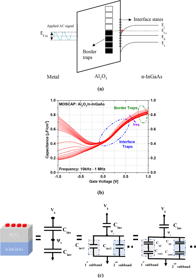
Border Trap Extraction with Capacitance- Equivalent Thickness ...
B Ideal MOS Capacitor

Electronic Devices: MOS Capacitor (06) - Threshold Voltage and Inversion charge

Energy band diagram of an MOS capacitor and operating regions ...
Lecture 14: MOSFETs

MOS Capacitor | Working Principle | 2+ Important parameters

Problem 6: The energy band diagram for an ideal MOS-capacitor ...
Electrical Characteristics of MOS Devices • The MOS Capacitor ...
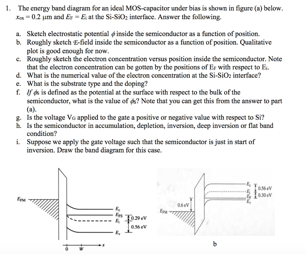
Solved 1. The energy band diagram for an ideal MOS-capacitor ...

mosfet - MOS Capacitor Band Edges - Electrical Engineering ...
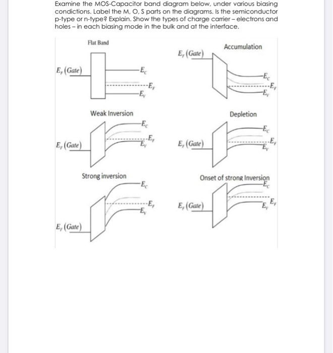
Examine the MOS-Capacitor band diagram below, under | Chegg.com

Gate Bias - an overview | ScienceDirect Topics

Lecture 15 OUTLINE The MOS Capacitor Energy band diagrams ...

Energy band diagram of MOS capacitor illustrating various ...
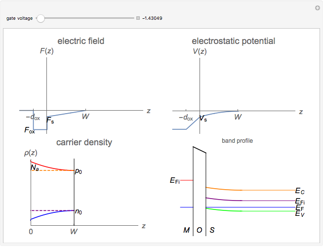
Applied Voltage on an Ideal MOS Capacitor - Wolfram ...
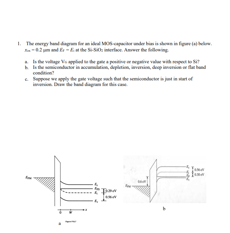
Solved The energy band diagram for an ideal MOS-capacitor ...
What is the concept of 'flat band voltage' in MOSFET devices ...
Distribution of Interface States in MOS Systems Extracted by ...

MOS Capacitor | MOS Capacitance C V Curve | Electrical4U
Lecture 14: MOSFETs

Band diagram of n-type MOS capacitor biased in (a ...
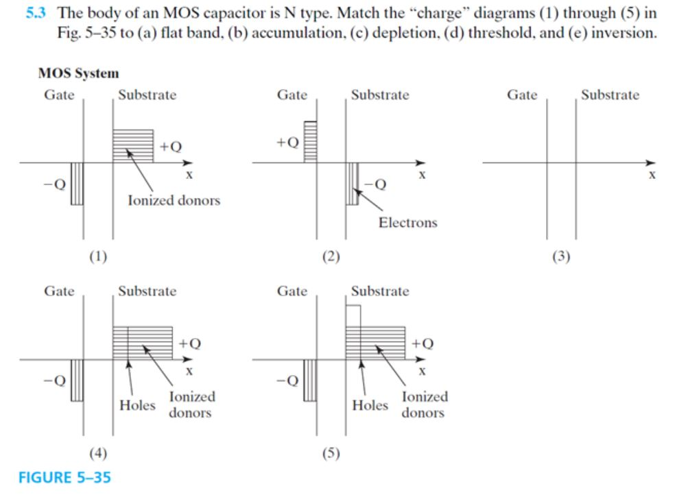
Solved 5.3 The body of an MOS capacitor is N type. Match the ...

Energy band diagram of an MOS capacitor and operating regions ...

The MOS capacitor. (a) Physical structure of an n+-Si/SiO2/p ...
![Solved [Q-3] (10 points) An MOS capacitor structure was ...](https://media.cheggcdn.com/study/914/914ec131-e923-4e8f-b690-3d7b325ef74d/image.png)
Solved [Q-3] (10 points) An MOS capacitor structure was ...

The MOS capacitor. (a) Physical structure of an n+-Si/SiO2/p-Si MOS capacitor, and (b) cross section (c) The energy band diagram under charge neutrality.
Automated drawing of the MOS band diagram

MOS Capacitor - University of California, Berkeley Pages 1-38 ...
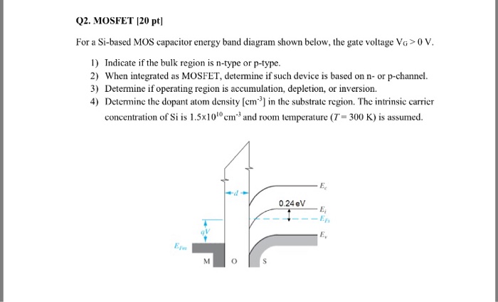
Solved Q2. MOSFET 120 ptl For a Si-based MOS capacitor ...
0 Response to "39 mos capacitor band diagram"
Post a Comment