37 how to draw energy band diagram
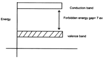
2. Energy Bands 3. e/h Current Energy Diagrams 21 Energy band diagram shows the bottom edge of conduction band, Ec, and top edge of valence band, Ev. Ecand Evare separated by the band gap energy, Eg. Electrons and holes tend to seek their lowest energy positions, electrons tend to fall in energy band diagram, holes float up like bubbles in water. Draw the energy band diagrams of p-type and n-type semiconductors. A semiconductor has equal electron and hole concentration 6 x 10⁸ m–3. Rating: 4,4 · 740 votes · Free · Android · Educational
22:41Hey Comrades! This is the complete video on the Energy Band Diagram concept. It will help you learn method ...20 Jul 2021 · Uploaded by Last Bencher Comrade
How to draw energy band diagram
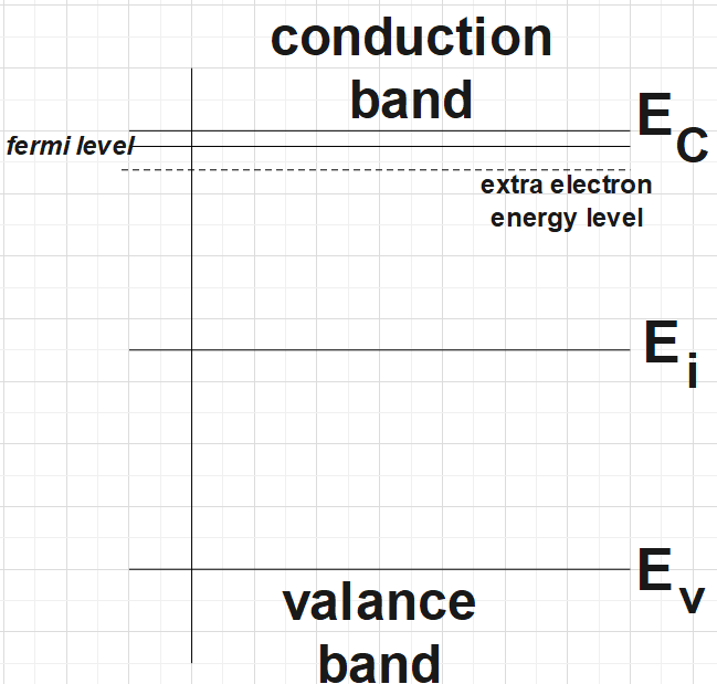
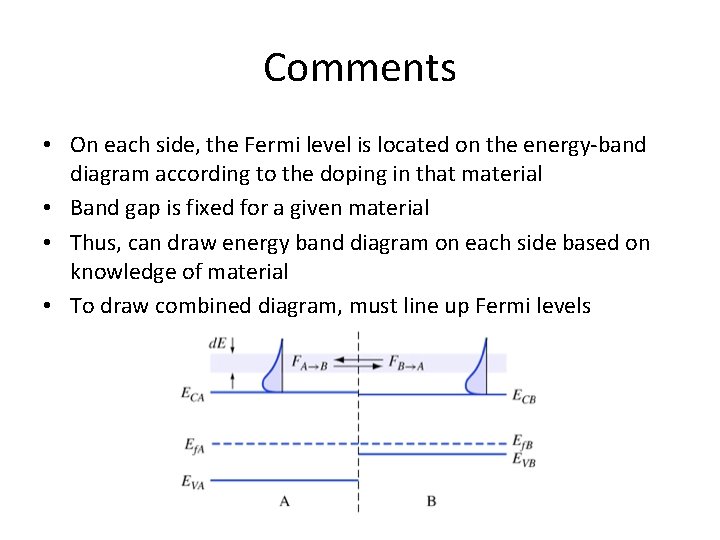
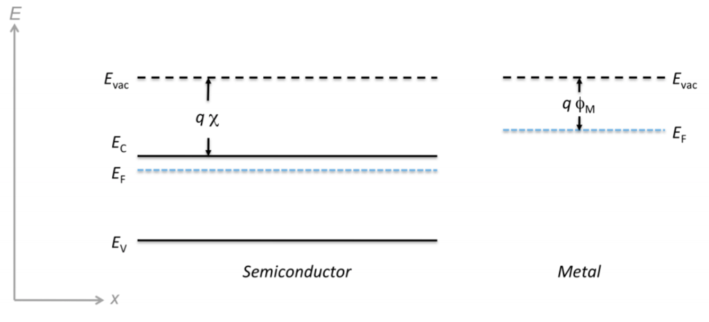
5:59In this tutorial I show how to sketch band diagrams for metals, insulators, and semiconductors. I also show how ...13 Mar 2018 · Uploaded by Taylor Sparks Draw and explain energy band diagram of MOS capacitor in accumulation, depletion and inversion region. ... The energy band diagram contains the electron energy levels in the MOS structure as deliniated with the fermi energy in the metal and semiconductor as well as the conduction and valence band edge in the oxide and the silicon. For a p-n junction at equilibrium, the fermi levels match on the two sides of the junctions. Electrons and holes reach an equilibrium at the junction and form a depletion region.The upward direction in the diagram represents increasing electron energy. That implies that you would have to supply energy to get an electron to go up on the diagram, and supply energy to get a hole to go down.
How to draw energy band diagram. Draw separate energy band diagrams for conductors, semi-conductors and insulators and label each of them. Answer. Verified. 54.9k+ views. Hint: Understanding about the valence band, conduction band and forbidden band will help to draw the energy band diagram of each material. Conductors don’t have forbidden band gaps. 1.04 Energy band diagrams. Energy has to be supplied to move electrons away from the nucleus of the atom. The valence electrons have the highest energy levels of the electrons that are still bound to their parent atoms, (as they are furthest from the nucleus). Additional energy is required to completely remove an electron from the atom, so free electrons have higher energy levels than valence ... Draw the energy band diagram of the | Chegg.com. 30 points 2. Draw the energy band diagram of the n/p/n" bipolar junction transistor under the following biasing conditions. Clearly show Ef, and Efp relating to Ec and Ey, respectively. Note that the n emitter is heavily doped and n* collector is lightly doped. ht n h +. Question: 30 points 2. you can easily draw your energy band diagram with few minute. Follow step: open Microsoft Word..go insert window...shapes.. New Drawing canvas. Good luck.10 answers · Top answer: Dear Ashraful The bandlab package LmtArt can draw the energy valence bands downloadable from ...
9:42Draw the energy band diagram of a p-type semiconductor. Deduce an expression for the conductivity of a p ...2 Aug 2020 · Uploaded by Doubtnut Energy band diagrams Lundstrom: Fall 2019 An energy band diagram is a plot of the bottom of the conduction band and the top of the valence band vs. position. Energy band diagrams are a powerful tool for understanding semiconductor devices because they provide qualitative solutions to the semiconductor equations. 15:57Electronic Devices: Energy band diagram concepts. 81,721 views81K views. May 7, 2015. 672. 26. Share ...8 May 2015 · Uploaded by techgurukula
Drawing energy band diagrams. I'm studying for a course in semiconductor devices, involving pn-diodes, schottky-diodes and mosfet transistors. Just wondering if there's any good online resource that demonstrates specifically how to draw energy band diagrams for the various devices in various situations (applied voltages, inversion, accumulation ... Energy levels — In solid-state physics of semiconductors, a band diagram is a diagram plotting various key electron energy levels as a function of some ... This quick video will give you a complete analysis of energy band diagram of pn juction diode. This quick video will give you a complete analysis of energy band diagram of pn juction diode. For a p-n junction at equilibrium, the fermi levels match on the two sides of the junctions. Electrons and holes reach an equilibrium at the junction and form a depletion region.The upward direction in the diagram represents increasing electron energy. That implies that you would have to supply energy to get an electron to go up on the diagram, and supply energy to get a hole to go down.
Draw Energy Band Diagrams Of An Ntype And Ptype Semiconductor Class 12 Physics Cbse
Draw and explain energy band diagram of MOS capacitor in accumulation, depletion and inversion region. ... The energy band diagram contains the electron energy levels in the MOS structure as deliniated with the fermi energy in the metal and semiconductor as well as the conduction and valence band edge in the oxide and the silicon.

Energy Band Diagram Revision Ppt Download
5:59In this tutorial I show how to sketch band diagrams for metals, insulators, and semiconductors. I also show how ...13 Mar 2018 · Uploaded by Taylor Sparks

Energy Band Diagram Of P Type And N Type Semiconductor Youtube

Draw Energy Band Diagram Of P N Type Semiconductors Also Write Two Differences Between P And N Type Semiconductors

Draw The Energy Band Diagrams Of I A Metal And Ii A Semiconductor

Draw Energy Band Diagram Of Intrinsic Semiconductor At T 0k And At T Gt 0k Diagram Plz Brainly In
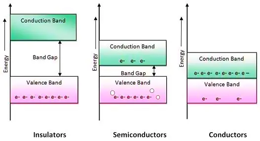
Material Classification Based On Energy Band Diagram Electricalvoice
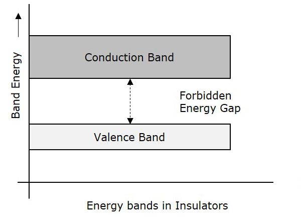
Draw A Labelled Energy Band Diagram For A Solid Which Is An Insulator What Is The Main Difference Between This Diagram And That Of A Semiconductor From Physics Conductors Insulators And Semiconductors

Draw Energy Band Diagram For Semiconductor And Metal Brainly In
What Is P Type Semiconductor Energy Diagram Conduction Examples

Draw The Energy Band Diagram Of I N Type And Ii P Type Semiconductors At Temperature T 0 K In The Case Of N Type Si Semiconductor The Donor Energy Level Is Slightly Below The Bottom Of Conduction Band Whereas
Draw Energy Band Diagrams Of N Type And P Type Semiconductors At Temperature T 0 K Mark The Donor And Acceptor Energy Levels With Their Energies Cbse Class 12 Physics Learn Cbse Forum
Nonhomogeneous Semiconductors Constancy Of The Fermi Level At
Draw The Energy Band Diagram When Intrinsic Semiconductor Ge Is Doped With Impurity Atoms Of Antimony Sb Sarthaks Econnect Largest Online Education Community

Energy Band Diagram Of Forward Biased Pn Junction Physics Stack Exchange

2 Energy Band Diagram For Gaas 5 Download Scientific Diagram
Draw Energy Band Diagram For P Type Semiconductor
Solved A Draw The Equilibrium Energy Band Diagram For An Chegg Com
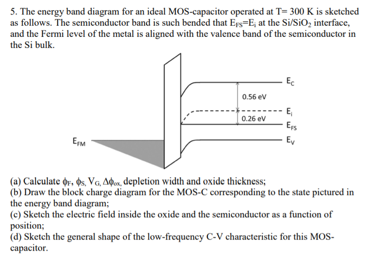
Solved 5 The Energy Band Diagram For An Ideal Mos Capacitor Chegg Com

Energy Band Diagram An Overview Sciencedirect Topics

Draw Energy Band Diagrams Of An N Type And P Type Semiconductor At Temperature T Ok Mark The Donor And Acceptor Energy Levels With Their Energies A Semiconductor Has Equal Electron And Hole
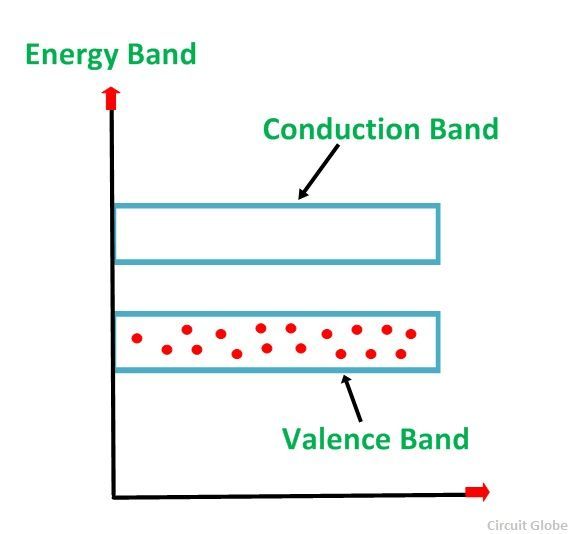
Basic Electronics Energy Bands

Draw The Energy Band Diagrams Of A Pn Junction When It Is I Under Equilibrium Ii Forward Biased Iii Reverse Biased Ask To Lecturenotes
What Is P Type Semiconductor Energy Diagram And Conduction Circuit Globe

Draw Separate Energy Band Diagram For Conductors Semi Conductors And Insulators And Label Each Of Them Physics Theory Shaalaa Com
Draw The Energy Bands Diagrams For A I Pure Semiconductor Ii Insulator How Does The Energy Sarthaks Econnect Largest Online Education Community
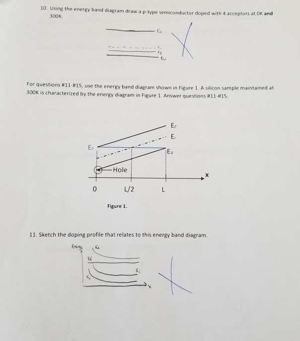
Solved 10 Using The Energy Band Diagram Draw A P Type Chegg Com

Draw The Energy Band Diagram Of An Intrinsic Semiconductor Youtube
Solved Metal Contact Semiconductor Energy Band Diagram Chegg Com

File Energy Band Diagram Svg Wikimedia Commons
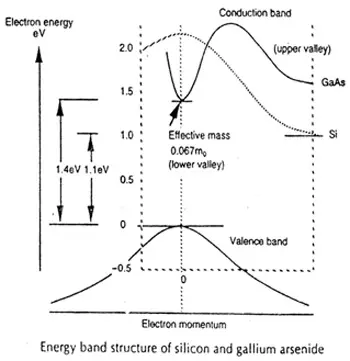
Gallium Arsenide Gaas Energy Band Structure Energy Band Diagram

Draw The Energy Bands Diagram For A I Pure Semiconductor Ii Insulator How Does The Energy Band Foe A Pure Semiconductor Get Affected When This Semiconductor Is Doped With An Acceptor Impurity
Simplified Energy Band Diagram Of A P N Junction A At Equilibrium And Download Scientific Diagram

Energy Bands Of Silicon Electrical4u

Draw Energy Band Diagram For N Type Semiconductor P Type Semiconductor Physics Semiconductor Electronics Materials Devices And Simple Circuits 9818193 Meritnation Com

The Energy Band Diagram Of An N Zno P Si Uv Photodiode Under A Download Scientific Diagram
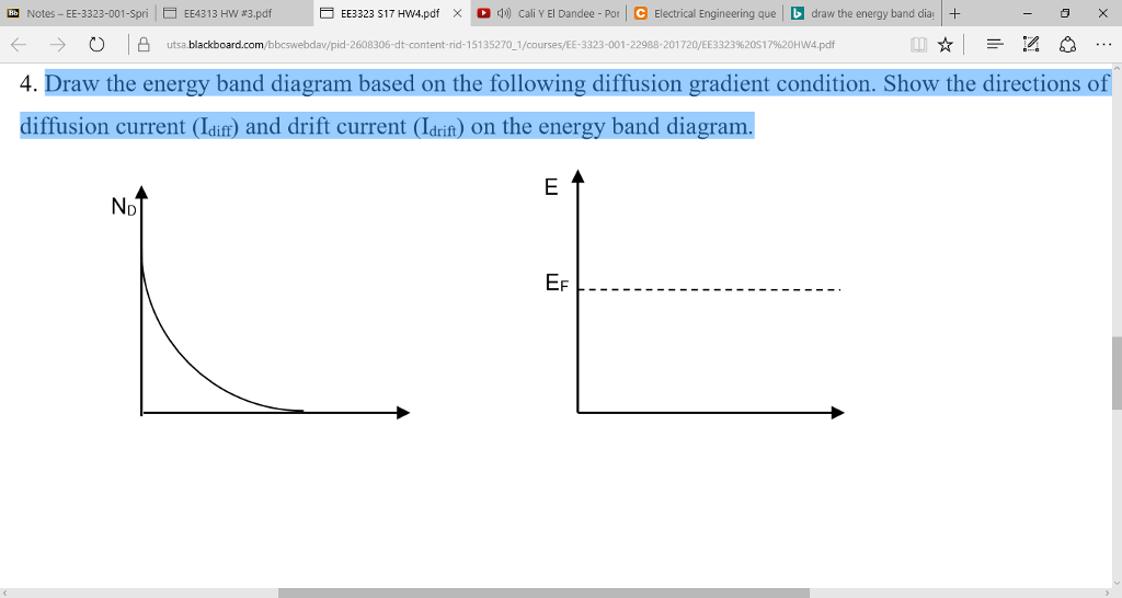
Solved Draw The Energy Band Diagram Based On The Following Chegg Com
0 Response to "37 how to draw energy band diagram"
Post a Comment